Item |
Manufacturer |
Part No. |
Supplier |
Supplier's Part No |
QTY |
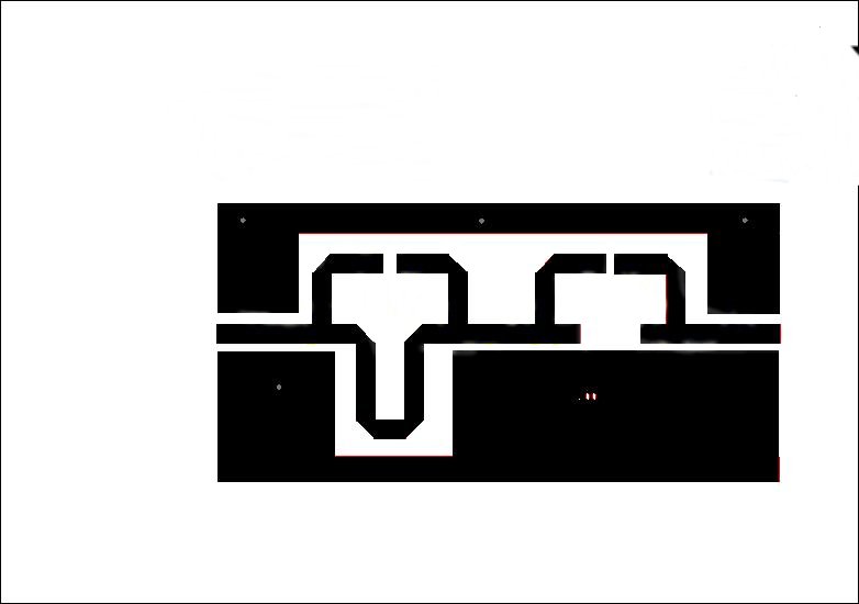
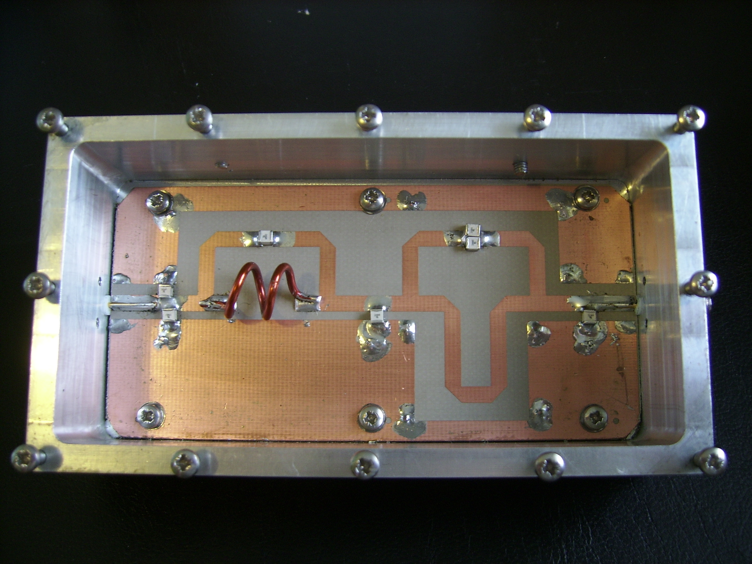
PCB |
Homemade |
Homemade |
Homemade |
1 |
|
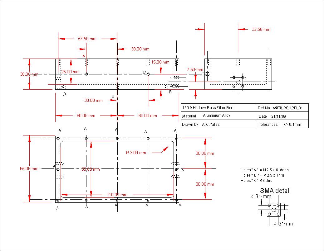
SMA Socket |
Various |
FEC |
105 - 6376 |
2 | |
M2.5 x 6 mm |
Various |
FEC |
142 - 0030 |
26 |
|
M2.5 washer |
Various |
FEC |
161 - 4000 |
18 |
|
M3 x 6 mm |
Various |
FEC |
142 - 0032 |
2 |
|
M3 Washer |
Various |
FEC |
161 - 4001 |
2 |
|
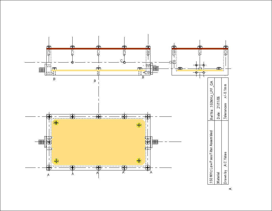
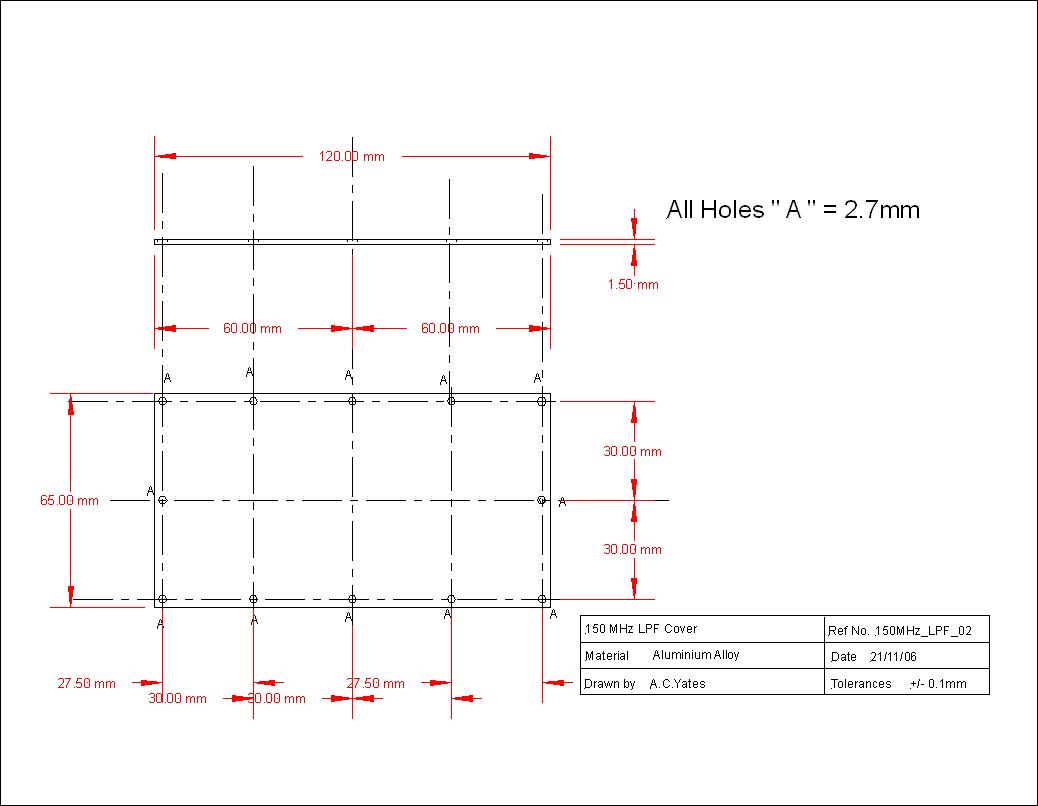
Lid |
Homemade |
1 |
|||
Case |
Homemade |
1 |
|||
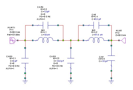
Capacitor |
ATC |
ATC100A1R2BT150X |
RS |
611 - 4335 |
1 |
Capacitor |
ATC |
ATC100A3R9BT150X |
RS |
611 - 4666 |
1 |
Capacitor |
ATC |
ATC100B4R7BT150X |
RS |
611 - 4868 |
1 |
Capacitor |
ATC |
ATC100B6R8BT150X |
RS |
611 - 4688 |
1 |
Capacitor |
ATC |
ATC100B8R2BT150X |
RS |
611 - 4964 |
2 |
Inductor |
Homemade |
1 |
|||
Supplier codes |
RS is RS Components |
FEC is Farnell Electronic Components |
|||
This page last updated 25th Oct 2009